
Press Release
WarRin Protocol: A point-to-point anonymous privacy communication system
Dr.WarRin
Summary
This white paper provides an explanation of the WarRin protocol and related blockchain, point-to-point, network value, transport protocol, and encryption algorithms. The limited space will highlight the WRC allocation scheme and purpose of the WarRin Protocol Token, which is important for achieving the WRC’s stated objectives. This white paper is for informational purposes only and is not a promise of final implementation details. Some details may change during the development and testing phases.
1. Introduction
Traditional centralized communication systems such as WeChat,WhatsApp, FacebookMessage,Google Allo,Skype face a range of problems, including government surveillance, privacy breaches, and inadequate security, and the WarRin protocol proposes apoint-to-pointencrypted communications system that leveragesblockchain technology, combined with Double Ratc het algorithms, pre-keys, and extended X3DH handshakes. The WarRin Protocol uses The Generalized Directional Acyclic Graph and Curve25519,AES-256, and HMAC-SHA256 as the pronamor, allowing each account to have its own unique account chain, providing unlimited instant communication between points and unlimited scalability, anonymity, integrity, consistency, and asynchronousness.
2. WarRin Protocol communication system
2.1 Two types of communication
The Waring Protocol communication system divides chat channels into two types.

Two modes of communication
- General Chat mode: Using point-to-point encrypted communication, the service side has access to the key and can log in via multiple devices.
- Secret Chat mode: Encrypted communication using point-to-point can only be accessed through two specific devices.
The design combines some of the advantages of raiBlocks multi-chain construction with IOTA/Byteball DAG, which we call the Waring protocol. With improvements, we have given the WarRin protocol greater throughput and faster processing power while ensuring the security of the ledger, and network nodes can store the ledger in less space and search their communications accounts quickly in the ledger. When two users communicate, third parties contain content that neither manager can access. When a user is chatting in secret, the message contains multimedia that can be designated as a self-destruct message, and when the message is read by the user, the message is automatically destroyed within the specified time. Once the message expires, it disappears on the user’s device.
2.2 How chat history is encrypted
2.2.1 MTProto Transport Protocol

MTProto transport protocol
The WarRin communication system draws on RaiBlocks’ multi-chain structure for point-to-point communication. Each account has its own chain that records the sending and receiving behavior of the account. For example, in Figure 1, there are 7 accounts, each with 7 chain records of the account sending and receiving communications. On the graph, horizontal coordinates represent the timeline, and portrait coordinates represent the index of the account.
Transferring information from one account to another requires two transactions: one to send a communication from the sender’s transfer content, and one to receive information to add that content to the content of the receiving account. Whether in a send-side account or a receiving account, a PoW proof of work with the previous communication content Hash is required to add new communications to the account. In the account chain, poWwork proves to be an anti-spam communication tool that can be done in seconds. In a single account chain, the Hash field of the previous block is known to pre-generate the PoW required for subsequent blocks. Therefore, as long as the time between the two communications is greater than the time required to generate the PoW, the user’s transaction will be completed instantaneously.
In such a design, only the receiving end of the communication is required for settlement. The receiving end places the received communication signature on the account chain, which is called accepted communication. Once accepted, the receiving end then broadcasts the communication to the ledger of the other nodes. However, there may be situations where the receiving end is not online or is subject to a DoS attack, which prevents the receiving end from putting the receiving side communication on the account chain, which we call uncommoted transactions. The X symbol in Figure 1 represents an open transaction sent from Account 2 to Account 5.

Obviously, because only the sending and receiving sides of the communication are required to settle, such communication is very lightweight, all traffic can be transmitted in a UDP package and processed very quickly. At the same time, all communications in an account are kept in one chain, with great integrity, and the ledger can be trimmed to a minimum. Some nodes are not interested in spending resources to store the full communication history of the account; They are only interested in the current communications for each account. When an account communicates, its accumulated information is encoded, and these nodes only need to keep track of the latest blocks so that historical data can be discarded while maintaining correctness. Such communication is only possible if the sending and receiving sides trust each other and are not the final settlement of the entire network consensus. There is a security risk in the absence of trust on the sending and receiving ends, or in situations where the receiving end is attacked by DoS without the sender’s knowledge.
We have observed that although each account has a separate chain, the entire ledger can be expressed in the form of a WarRin object. As shown in Figure 2, this is represented by the WarRin astros trading on all accounts in Figure 1.

The first unit in the WarRin object is the Genesis unit, the next six cells represent the allocation of the initial token, and the other units correspond to the communication transactions between the account chains. We use the symbol a/b to represent a communication transaction, where the sender is a andthe recipient is b. The last 4/1 unit in Figure 2 is the last communication corresponding to Figure 1 – sending communication from account 4 to account 1. A transaction in Figure 1 is a confirmation of the latest block or the latest communication on the account chains of both parties to the communication, reflected in Figure 2 as a reference to the latest units of the account chains of both parties to the communication. Take unit 4/1, for example, where the latest block on account 4 was the receiving block for 2/4 trades and the newest block on account 1 was the send block for 1/5 trade. So on the DAG, the 4/1 cell refers to the 2/4 cell and the 1/5 cell.
The WarRin protocol uses triangular shrapned storage technology to crack impossible triangles in the blockchain through the shrapghine technology, with extensive node engagement and decontalination while maintaining high throughput and security:
- Complete shraping of blockchain status;
- Secure and low-cost cross-synth trading;
- Completely random witness selection;
- Flexible and efficient configuration
Complete decentralization ensures absolute security and scalability of the standard chain.
(Figures above show seven Ling-shaped objects:2/1 one;3/2 one… )
2.2.2 Curve25519 Elliptic Curve Encryption Algorithm
Curve25519, proposed by Daniel Bernstein, is anelliptic curve algorithm for the exchange of The Montgomery Curve’s Difi Herman keys.
Montgomery Curve Curve Mathematical Expression:
Curve25519 Curve Mathematical Expression:
Curve25519 encryption algorithms are used for standard private and public keys, and the private keys used for Curve25519
encryption algorithms are typically defined as secret
indices, corresponding to
public keys, coordinate points, which are usually sufficient to perform ECDH (elliptical) and symmetrical elliptic curve encryption algorithms. If one party wants to send information to the other party and the other party has the
public
and private keys, perform the following
calculation:
Generate a one-time random secret
index, calculated using Montgomery, because the message is a symmetrical password encrypted using 256-bit sharing, such as AES using a 256-bit integer
one-time public key, as akey, and 256-bit integer is a
prefix to encrypted information. Once a party to
the public
key receives this message, it can start by calculating , that is ,
the receiver recovers the shared secret and
is able to decrypt the rest of the information.
3. Incentives
On the basis of the WarRin agreement, by adding the incentive layer, we can effectively avoid the whole network being attacked and eliminate spam. As long as honest nodes control most of the calculations, for an attacker, the network is robust because of its simplicity of structure, and nodes need little coordination to work at the same time. They do not need to be authenticated because information is not sent to a location.
3.1 WRC Certificate
WRC issued a total of 2,500,000 pieces and continued to increment according to the WoRin gain function.
3.1.1 WoRin Gain Function


3.1.2 WoRin gain function control table
| The WoRin gain function is compared to the table | ||
| Number of layers /F | Growth factor /I | WRC circulation |
| [1,50] | 0.002 | 334918.8057 |
| [51,100] | 0.002 | 780024.2108 |
| [101,150] | 0.004 | 1177129.617 |
| [151,200] | 0.006 | 1487860.923 |
| [201,250] | 0.01 | 1722637 |
| [251,300] | 0.016 | 1894309.216 |
| [301,400] | 0.03 | 2101623.789 |
| [401,500] | 0.06 | 2217555.464 |
| [501,1000] | 0.1 | 2450712.257 |
| [1001,2000] | 0.12 | 2557457.3 |
According to the Gain function, the
larger the number of layers,
the greater the growth rate, the faster each layer is filled, and the
greater the circulation.
3.2 Allocation

WarRin protocol node distribution
3.2.1 Node allocation
Set the initial price
to 0.02,the layer where the first node is located is , according to the equation of the iso-difference column, there is , so that the
node token is assigned to the piece, for the price of
the layer where the node
is located, there is a
set.
For example, the number of tiers in which the 98th node is located is Tier 13, and the price of Tier 13 is 0.214,the tokens assigned by Tier 98 are
3.2.2 Total number of address assignments
Each node occupies one address, and the total number of addresses is
4. The use
WRC is the native pass-through of the WarRin protocol, andWRC will assign to Genesis nodes according to the above allocation scheme, which together form the entire network, andWRC can be used in the following scenarios, including but not limited to:
Pay the network’s gas charges, i.e. for transferring money and invoking smart contracts;
System Staking tokens, used for node elections and token issues;
The capital is lent to the validator in exchange for the amount of the reward;
Voting rights for system proposals;
The means of payment for apps developed on WoRin Services;
WoRin Storage is a means of payment on the decentralization storage;
WoRin DNS domain name and WoRin WWW website means of payment;
WoRin Proxy agents hide the means of payment for body and IP addresses;
WoRin Proxy penetrates payment methods reviewed by local ISPs
……
5. Conclusions
Metcalfe’s Law states that thevalue of a network is equal to the square of the number of nodes within the network, and that the value of the network is directly related to the square of the number of connected users. That is ( the
value factor, the number of
users.) That is, the greater the number of users on a network, the greater the value of the entire network and each computer within that network. The WarRin protocol also follows this law, and when the number of nodes reaches a certain level, the entire network becomes more robust.
References
[1] K. Birman, Reliable Distributed Systems: Technologies, Web Services and
Applications, Springer, 2005.
[2] V. Buterin, Ethereum: A next-generation smart contract and de- centralized
application platform, https://github.com/ethereum/wiki/wiki/White-Paper, 2013.
[3] M. Ben-Or, B. Kelmer, T. Rabin, Asynchronous secure computa- tions with
optimal resilience, in Proceedings of the thirteenth annual ACM symposium on
Principles of distributed computing, p. 183–192. ACM, 1994.
[4] M. Castro, B. Liskov, et al., Practical byzantine fault tolerance, Proceedings of the
Third Symposium on Operating Systems Design and Implementation (1999), p. 173–
186, available at http://pmg.csail.mit.edu/papers/osdi99.pdf.
[5] EOS. IO, EOS. IO technical white paper,
https://github.com/EOSIO/Documentation/blob/master/TechnicalWhitePaper.md,
2017.
[6] D. Goldschlag, M. Reed, P. Syverson, Onion Routing for Anony- mous and
Private Internet Connections, Communications of the ACM, 42, num. 2 (1999),
http://www.onion-router.net/Publications/CACM-1999.pdf.
[7] L. Lamport, R. Shostak, M. Pease, The byzantine generals problem, ACM
Transactions on Programming Languages and Systems, 4/3 (1982), p. 382–401.
[8] S. Larimer, The history of BitShares,
https://docs.bitshares.org/bitshares/history.html, 2013.
[9] M. Luby, A. Shokrollahi, et al., RaptorQ forward error correction scheme for
object delivery, IETF RFC 6330, https://tools.ietf.org/html/rfc6330, 2011.
[10] P. Maymounkov, D. Mazières, Kademlia: A peer-to-peer infor- mation system
based on the XOR metric, in IPTPS ’01 revised pa- pers from the First International
Workshop on Peer-to-Peer Systems, p. 53–65, available at
http://pdos.csail.mit.edu/~petar/papers/ maymounkov-kademlia-lncs.pdf, 2002.
About Author
Disclaimer: The views, suggestions, and opinions expressed here are the sole responsibility of the experts. No Digi Observer journalist was involved in the writing and production of this article.

Community Walk Benefiting the Empower Play Campaign Will Bring Families, Advocates, and Community Leaders Together to Celebrate Inclusion, Accessibility, and Belonging for Neurodivergent Children and Families in Delaware and beyond.
Wilmington, Delaware, United States, 29th Jul 2026 — As families across Delaware continue to advocate for greater accessibility and inclusion, the Delaware Sensory Museum (DSM) is bringing the community together for Walk for Life, a family-centered event designed to raise awareness, expand access, and support sensory-friendly experiences for neurodivergent children and their families.
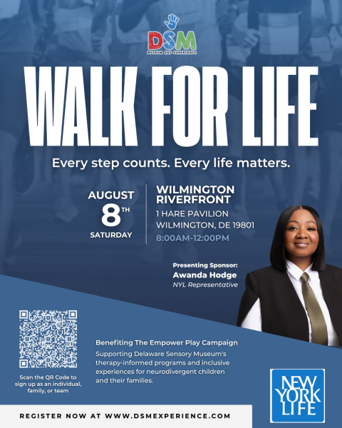
The walk will take place on Saturday, August 8, 2026, from 8:00 a.m. to 12:00 p.m. at 1 Hare Pavilion on the Wilmington Riverfront and will benefit DSM’s Empower Play Campaign, an initiative dedicated to creating more inclusive play opportunities, sensory-friendly programming, educational resources, and community support for children and families throughout Delaware.
More than a fundraiser, Walk for Life is a community movement focused on celebrating neurodiversity and creating environments where every child has the opportunity to learn, play, connect, and thrive. The event will bring together families, educators, healthcare professionals, advocates, businesses, and community leaders for a morning centered on awareness, connection, and action.
Across Delaware, families continue to seek more inclusive environments where children of all abilities can safely play, learn, and build meaningful connections. Through the Empower Play Campaign, DSM is helping meet that need by expanding sensory-friendly experiences, increasing access to resources, and creating welcoming spaces where neurodivergent children and their families feel supported.
“As a mother and community advocate, I have seen firsthand the strength and resilience of families raising children with disabilities. That is why I am proud to support the Delaware Sensory Museum and its mission to create more inclusive opportunities for neurodivergent children and their families. The Walk for Life is more than a community event. It is a call to action to raise awareness, expand access, and ensure every individual is seen, supported, and empowered to thrive.” Awanda Hodge, presenting sponsor of Walk for Life
Participants and attendees will enjoy a morning filled with family-friendly activities, music, community resources, giveaways, prizes, and opportunities to connect with organizations that support neurodivergent individuals and their families. Families, community organizations, and supporters will walk together along the Wilmington Riverfront to demonstrate that inclusion starts with showing up.
As families across Delaware continue to advocate for greater accessibility and inclusion, DSM hopes Walk for Life: Every Step Counts becomes more than an annual event. The organization envisions it as a growing community movement that celebrates neurodiversity, strengthens families, and reminds every individual that they belong.
“At SIVAD, we believe every person deserves the opportunity to live healthier lives and reach their full potential. Our partnership with the Delaware Sensory Museum reflects our shared commitment to creating healthier, more inclusive environments for children and families. Supporting the Walk for Life is an investment in hope, innovation, and a future where every family has the opportunity to thrive.” Dustin Davis, VP of business development at Delaware Sensory Museum
Community members are encouraged to register, participate, volunteer, donate, or become sponsors. Every step helps create a more inclusive Delaware where children of all abilities have the opportunity to learn, play, and thrive. To register, check out the link here: https://givebutter.com/the-empower-play-campaign-rlboej?gbtid=4b998e23799048379c012bb584073040
Event Details:
What: Delaware Sensory Museum Walk for Life
When: Saturday, August 8, 2026
Time: 8:00 a.m. – 12:00 p.m.
Where: 1 Hare Pavilion, Wilmington Riverfront, Wilmington, DE 19801
Benefiting: Delaware Sensory Museum Empower Play Campaign
Media Opportunity:
Media are invited to cover Walk for Life, capture community engagement, interview DSM representatives, sponsors, participating families, and community advocates, and learn more about the Empower Play Campaign and its impact on Delaware families.
For media inquiries, contact:
Courtney Haywood
Courtney Haywood Agency
courtney@courtneyhaywoodagency.com
About Delaware Sensory Museum:
The Delaware Sensory Museum (DSM) is dedicated to creating inclusive, sensory-friendly experiences that celebrate neurodiversity and empower children and families. Through interactive programming, educational opportunities, advocacy, and community partnerships, DSM creates welcoming spaces where individuals of all abilities can learn, play, connect, and thrive. To learn more visit, https://www.dsmexperience.com/
Media Contact
Organization: Delaware Sensory Museum
Contact Person: Courtney Haywood
Website: https://www.dsmexperience.com
Email: Send Email
City: Wilmington
State: Delaware
Country:United States
Release id:47689
The post Delaware Sensory Museum Unites Community for Walk for Life to Expand Inclusive Play appeared first on King Newswire. This content is provided by a third-party source.. King Newswire makes no warranties or representations in connection with it. King Newswire is a press release distribution agency and does not endorse or verify the claims made in this release. If you have any complaints or copyright concerns related to this article, please contact the company listed in the ‘Media Contact’ section
About Author
Disclaimer: The views, suggestions, and opinions expressed here are the sole responsibility of the experts. No Digi Observer journalist was involved in the writing and production of this article.
Press Release
Apex Financial Ltd: Chief Strategic Analyst Christopher James Carter Unveils RWA-AI-Safeguards
Speaking on behalf of Apex Financial Ltd at a recent international fintech and artificial intelligence forum in London, Christopher James Carter presented the company’s RWA-AI-Safeguards framework, which organizes asset digitization, AI-supported research, human review, and predefined risk controls within a structured investment research process.
United States, 29th Jul 2026 – At a recent international fintech and artificial intelligence industry forum in London, Christopher James Carter, Chief Strategic Analyst at Apex Financial Ltd, spoke on behalf of the company about a research and governance methodology referred to as the RWA-AI-Safeguards framework. The presentation examined how the digital representation of real-world assets, agentic artificial intelligence, and predefined risk controls could be organized within a connected investment research workflow.

Rather than presenting artificial intelligence as a replacement for analysts or portfolio decision-makers, Carter described the framework as a way to divide responsibilities among data systems, analytical models, human reviewers, and risk-governance processes.
According to Apex Financial Ltd, the framework is intended to support more structured research and decision-making. It does not constitute a recommendation to purchase or sell any asset and does not guarantee investment outcomes.
Reassessing Existing Investment Research Workflows
During the presentation, Christopher James Carter discussed several operational challenges affecting modern investment research.
Financial institutions and market participants now process increasing volumes of pricing data, economic indicators, company information, market sentiment, and geopolitical developments. Although automated systems can process this information more quickly than manual methods, speed alone does not ensure that an analysis is accurate, complete, or appropriate for a particular market environment.
Carter identified three areas addressed by the framework: limitations affecting the transfer and administration of certain assets, the possibility of inaccurate or unsupported outputs from artificial intelligence models, and the limitations of risk reviews that occur only after a material market movement has taken place.
The RWA-AI-Safeguards methodology is designed to examine these issues as connected parts of one research process rather than as separate technology functions.
RWA as an Asset and Data Layer
The first component of the framework concerns real-world assets, commonly referred to as RWA.
Within financial technology, RWA structures generally involve digitally representing rights or interests associated with an underlying asset. Depending on the legal and operational arrangement, the underlying asset may include financial instruments, contractual rights, or other recognized economic assets.
Apex Financial Ltd’s framework considers how these digital representations may support more standardized recordkeeping, programmable transaction instructions, and clearer data exchange between systems.
The company does not assume that tokenization automatically creates liquidity or changes the legal settlement terms of an underlying asset. Ownership rights, custody arrangements, transfer restrictions, settlement timing, and investor eligibility remain subject to the structure of the asset, applicable agreements, service providers, and relevant laws.
Within the methodology, the RWA layer is therefore treated primarily as an asset-information and transaction-structure layer. Its purpose is to give analytical systems a more consistent set of information about ownership, valuation, transfer conditions, and other relevant asset characteristics.
Agentic AI in the Research Process
The second component introduces agentic artificial intelligence into defined areas of the research workflow.
Agentic AI generally refers to software agents designed to monitor selected information, complete assigned analytical tasks, and respond to predefined conditions with less continuous manual prompting than conventional software tools.
Within the RWA-AI-Safeguards framework, these agents may be used to organize market information, compare changing data points, identify unusual conditions, test alternative scenarios, and prepare analytical material for further review.
The framework does not treat AI-generated conclusions as independently authoritative. Carter explained that model outputs can be affected by incomplete information, unsuitable assumptions, data errors, changing market relationships, and so-called AI hallucinations.
For that reason, the methodology separates automated analysis from final human evaluation. Analysts remain responsible for assessing whether an output is supported by reliable data, whether the assumptions remain relevant, and whether additional review is necessary. This human-review layer is intended to reduce reliance on a single model or unverified analytical output.
Safeguards as a Risk-Governance Layer
The third component, Safeguards, establishes risk and governance boundaries around the analytical process.
These controls may include data-quality requirements, model-confidence thresholds, exposure limits, concentration parameters, liquidity assessments, escalation procedures, and rules requiring additional human review.
When a model produces an output that falls outside defined parameters, the framework may flag the result, pause the relevant analytical workflow, request additional data, or refer the matter to a designated reviewer.
Where the methodology is incorporated into a trading or portfolio-support environment, any resulting instruction remains subject to user authorization, applicable account agreements, third-party broker capabilities, liquidity, market conditions, and technical availability.
Risk parameters cannot prevent all losses or guarantee that an instruction will be executed at a particular price. Their role is to create documented boundaries within which research findings and potential actions can be evaluated.
Relationship to the Apex Nova Development Framework
Christopher James Carter also discussed how the RWA-AI-Safeguards methodology is informing the continuing development of Apex Nova, a financial technology environment being developed by Apex Financial Ltd. The planned architecture separates several functions that are often combined within a single automated process. These include asset-data organization, AI-supported analysis, human verification, user permissions, and risk monitoring.
According to the company, this separation is intended to make the origin and review status of analytical information easier to understand. Apex Nova is not described as an autonomous substitute for professional judgment. The development approach emphasizes that artificial intelligence can support data processing and scenario analysis, while users and qualified professionals remain responsible for reviewing information and making decisions within the terms applicable to their accounts.
Specific features, asset availability, integrations, and implementation timelines remain subject to development, testing, third-party arrangements, and applicable regulatory requirements.
Regulatory and Organizational Background
Apex Financial Ltd was established in 2021 and develops financial research, analytical, and risk-management technology.
Public records maintained through the Investment Adviser Public Disclosure database list Apex Financial Ltd under CRD No. 342652 and SEC file No. 802-136476 as an exempt reporting adviser.
Exempt reporting adviser status is a regulatory filing classification. It does not constitute approval, certification, endorsement, or verification by the U.S. Securities and Exchange Commission of the company, its technology, its services, or any investment methodology.
About Apex Financial Ltd
Apex Financial Ltd is a financial technology company developing research, data-analysis, asset-structure, and systematic risk-governance tools. Established in 2021, the company studies how real-world asset infrastructure, artificial intelligence, human analysis, and defined controls can be incorporated into structured financial research workflows.
Risk Disclosure
This release is provided for general informational purposes only. It does not constitute investment, legal, or tax advice, an offer to purchase or sell securities, or a recommendation to use any product, service, asset, or investment strategy.
Investment and securities trading involve risk, including the possible loss of principal. Tokenized asset structures, artificial intelligence, analytical models, automated systems, and risk controls do not eliminate investment risk or guarantee future performance.
Media Contact
Organization: Apex Financial Ltd
Contact Person: Henry Johnny
Website: https://apex-web.com/
Email: Send Email
Country:United States
Release id:47652
The post Apex Financial Ltd: Chief Strategic Analyst Christopher James Carter Unveils RWA-AI-Safeguards appeared first on King Newswire. This content is provided by a third-party source.. King Newswire makes no warranties or representations in connection with it. King Newswire is a press release distribution agency and does not endorse or verify the claims made in this release. If you have any complaints or copyright concerns related to this article, please contact the company listed in the ‘Media Contact’ section
About Author
Disclaimer: The views, suggestions, and opinions expressed here are the sole responsibility of the experts. No Digi Observer journalist was involved in the writing and production of this article.
Press Release
Dr. Angela Zeng Appears on The Breakfast Club to Discuss Traditional Chinese Medicine and Nutrition

Dr. Angela Zeng, Ph.D., MBA, founder and CEO of Karviva Wellness Beverages, recently appeared on The Breakfast Club, joining hosts Charlamagne Tha God and Jess Hilarious for a conversation about Traditional Chinese Medicine, nutrition, and the ideas explored in her debut book, The Balance Cure: The TCM Way to Lasting Weight Loss.
During the interview, Dr. Angela discussed the principles of Traditional Chinese Medicine and how they have influenced her work as a scientist, entrepreneur, and author. She also shared the inspiration behind The Balance Cure, which presents Traditional Chinese Medicine alongside modern nutritional science and invites readers to explore different perspectives on nutrition and lifestyle.
The conversation also touched on Karviva and the philosophy that has guided the company since its founding. Inspired by Traditional Chinese Medicine and contemporary nutrition research, Karviva develops plant-based beverages using thoughtfully selected ingredients.
“I appreciate opportunities to introduce more people to Traditional Chinese Medicine and to share the ideas that have shaped my work,” said Dr. Angela Zeng. “Conversations like these create space for people to explore different perspectives on nutrition and wellness.”
The interview follows several recent milestones for Dr. Angela and Karviva. Over the past year, her work has been featured in Bon Appétit, while Karviva’s Profit Cacao Whole Plant Protein & Prebiotic Smoothie was recognized in the 2026 Good Housekeeping Snack Awards.
The full interview is available through The Breakfast Club on the official iHeart platform.
About Dr. Angela Zeng
Dr. Angela Zeng, Ph.D., MBA, is a food scientist, medical scientist, Traditional Chinese Medicine scholar, and founder and CEO of Karviva. Born into generations of Chinese herbal practitioners and trained in pathology, biochemistry, and nutrition, she writes and speaks about Traditional Chinese Medicine, nutrition, and functional foods. She is the author of The Balance Cure: The TCM Way to Lasting Weight Loss.
About Karviva
Karviva is a St. Louis-based beverage company founded by Dr. Angela Zeng. Inspired by Traditional Chinese Medicine and modern nutritional science, the company develops plant-based beverages made with thoughtfully selected ingredients.
Media Contact
Organization: Karviva
Contact Person: Dr. Angela Zeng
Website: https://karviva.com/
Email:
angela@karviva.com
City: Saint Louis
State: Missouri
Country:United States
Release id:47124
The post Dr. Angela Zeng Appears on The Breakfast Club to Discuss Traditional Chinese Medicine and Nutrition appeared first on King Newswire. This content is provided by a third-party source.. King Newswire makes no warranties or representations in connection with it. King Newswire is a press release distribution agency and does not endorse or verify the claims made in this release. If you have any complaints or copyright concerns related to this article, please contact the company listed in the ‘Media Contact’ section
About Author
Disclaimer: The views, suggestions, and opinions expressed here are the sole responsibility of the experts. No Digi Observer journalist was involved in the writing and production of this article.
Delaware Sensory Museum Unites Community for Walk for Life to Expand Inclusive Play
Apex Financial Ltd: Chief Strategic Analyst Christopher James Carter Unveils RWA-AI-Safeguards
Dr. Angela Zeng Appears on The Breakfast Club to Discuss Traditional Chinese Medicine and Nutrition
Benzinga Money Article Discusses How to Become Part of the 12% of Retirees Who Have Achieved the Recommended $550,000 Minimum Retirement Savings Threshold
Apu Apustaja Conquers New York with Lively Street Ads, Including Times Square Billboard
Bay Smokes Maintains Quality Amid Legislative Changes in the Hemp Industry


-
Press Release5 days ago
Post Oak Group Advises on Successful Sale of Philadelphia-Based Computer Solutions Business to Search Fund-Backed Acquirer
-
Press Release5 days ago
Harborstone Point Advisors Expands Revenue Cycle Management and Financial Advisory Services for Behavioral Health Organizations
-
Press Release4 days ago
All Thingz Electric Expands EV Charger Installation Services Across South Orange County to Meet Growing Demand
-
Press Release5 days ago
Anime Expo 2026 Jaadugar A Witch in Mongolia Reveal Behind-the-Scenes Insights and Anime Secrets
-
Press Release4 days ago
RELVE Q2 Report Reveals AI Hype Gap After Analyzing 1.59M Data Points and 23,000 Tools
-
Press Release4 days ago
23 Years, One Question: “Diaoyu Dao: Small Islands, Big Stakes” — A CGTN Documentary
-
Press Release3 days ago
Biomaser and LatinLook Strengthen PMU Partnership in Argentina
-
Press Release4 days ago
Ken Behr Turns Years as a DEA Cooperating Source Into True Crime Podcast Crime Nightly