
Press Release
Project PAI Announces Technical Progress, Catena NFT Platform is Coming Soon!
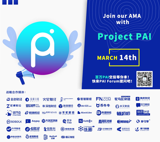
The annual PAI Day on March 14, 2021 came as usual. To thank PAI enthusiasts for their continued support, Project PAI core developers launched an AMA campaign through the community and gave millions of airdrop rewards back to PAI contributors and community members. The following are the selected AMA questions, enjoy:
Q: Why do I feel like the Project PAI Team has been quiet for a while? What has been done by Project PAI in the past year? What is the recent work plan done by Project PAI? Will there be plans to support DeFi and NFT?
A: In October 2020, PAI switched from a conventional PoW-style blockchain to a new PoW/PoS Hybrid Consensus model. The current primary focus of the PAI Core Contributors is to ensure that the PAI blockchain is stable and reliable, so that PAI Hybrid Consensus can thrive as a fully decentralized network In addition to technical contributions, this includes acquiring more network participants to further decentralize the blockchain, and providing support to the Catena NFT project, which will soon support PAI Coins and enable Project PAI ecosystem.
The team is following up on the trends in the Defi world, and will participate in the innovation of the Defi world by cooperating with other projects. In addition, we are studying possible technical solutions to enable cross-chain features for PAI coins (such as Ethereum, Heco, BSC, etc.), which enables PAI coins to be used in some Defi applications in the future.
Q: When will Project PAI’s NFT platform go online? Compared with other NFT trading platforms on the market (such as OpenSea, Rariable, etc.), what are the advantages?
A: The Catena NFT platform based on the PAI blockchain is currently available on catenaart.com and is currently in the public prototype testing stage, allowing people to upload their own arts on the platform. The core contributors of PAI sincerely welcome you to participate in the prototype test of the product and provide any suggestions or feedback. After completing the prototype test, we will further optimize the product and improve the user experience design based on the feedback. The first official version is expected to be released in Q2 of 2021.
Cartena NFT is a completely decentralized art trading platform based on the PAI blockchain. The main features of Cartena NFT are:
1. Fully decentralized NFT trading market, connecting on-chain and off-chain: On Cartena NFT platform, you not only trade NFT, but also obtain its NFT on the PAI blockchain while trading real arts, which is both on-chain and off-chain.
2. Support multiple payment channels: Catena NFT platform will support PAI coins, mainstream cryptocurrencies (BTC, ETH, etc.) and credit card payments.
3. The built-in encrypted communication system allows the buyer and seller to communicate during the NFT transactions to ensure the progress of each transaction.
4. The identity authentication system based on PAI PASS ensures the authenticity of both parties in the market. Users can track each step of each transaction on the PAI blockchain.
Welcome to participate in the prototype test of Cartena NFT platform and give feedback on the PAI forum.
Test url: https://catenaart.com/
Q: What is PAI’s PoUW? When is it planned to launch?
A: Project PAI’s Proof of Useful Work (PoUW, Proof of Useful Work) is a research project designed to enable miners to perform machine learning calculations while verifying PAI currency transactions. The purpose of PoUW is to use AI calculations to replace traditional PoW hashing operations, so that the computing power on the blockchain can be used for actual AI applications, making these computing powers “useful”. In the future, these computing powers can not only be used for machine learning training, but can also be extended to general-purpose on-chain computing, such as on-chain data analysis, cryptographic-based on-chain privacy computing (such as zero-knowledge proof, secure multi-party computation), etc.
PoUW is a passionate research-oriented project, completed by multiple core contributors to Project PAI. The PoUW testnet was originally planned to be launched in the second half of 2021. Due to the cutting-edge and uncertainty of technical research and other product plans of Project PAI, we will try our best to ensure the launch of the PoUW testnet.
For the latest progress, you can check:
Project Page:
https://projectpai.com/pai-research/
Github repo :
https://github.com/projectpai/pouw-main-iteration
Q: The current applications and use cases for PAI seem unclear to me. What does PAI’s economy offer compared to other chains that focus on use cases like finance?
A: Referencing the original vision (tech white paper), the PAI Blockchain fundamentally comprises three modules: Authentication layer, Blockchain layer, and Data layer:
1.The Authentication layer controls relationships that exist in the PAI ecosystem.
2.The Blockchain layer houses a record of network transactions as well as protocols for peer-to-peer engagement.
3.The Data layer indexes encrypted data, peer-to-peer, with hashed references.
Theoretically, any applications or use cases which require one or a combination of authentication services, transactional services, or data storage and sharing services (which, as you can imagine, is quite a lot) can leverage PAI blockchain technology. Currently, the most concrete example of a PAI use case is the NFT art platform, Catena, which is accessible at catenaart.com.
We will release other questions in the PAI weekly newsletter one by one. Welcome to pay attention to the wechat public account of Project PAI and PAI Fans, and keep track of the latest progress of the project. Thank you for your continued support!
Following Project PAI:
Project PAI official website: https://projectpai.com/
PAI Forum:https://www.paiforum.com
Project PAI wechat public account:Project PAI
PAI fans wechat public account:PAIFans
Cartena NFT: https://catenaart.com/
PAI Coin Pool : https://paicoinpool.com
PAIUp wallet: https://www.paiup.com
Join our global community:
Telegram(English): https://t.me/projectpai
Telegram(Chinese): https://t.me/projectpaiCN
Telegram(Korean): https://t.me/ProjectPAIKoreaOFFICIAL
Telegram(Japanese): https://t.me/ProjectPAIJapanOFFICIAL
Twitter: https://twitter.com/projectpai
Facebook: https://www.facebook.com/projectpai
Medium: https://medium.com/project-pai
Youtube: https://www.youtube.com/c/projectpai
Reddit: https://www.reddit.com/user/projectpaiofficial/
About Author
Disclaimer: The views, suggestions, and opinions expressed here are the sole responsibility of the experts. No Digi Observer journalist was involved in the writing and production of this article.

How to easily earn dollars has become the focus of many people. Now, a brand new opportunity is quietly coming – DN Miner! Whether you are a newcomer in the workplace or an experienced investor, this platform opens a door to wealth for you. Seize the opportunity, change your destiny, and make your time and efforts truly profitable!
- After the user registers, you can get $100 from the platform. No need to wait, start your money-making journey immediately!
- Choose a solution contract that suits your needs and budget. After the purchase is completed, the contract will officially take effect, and you can start to enjoy the fun of making money.
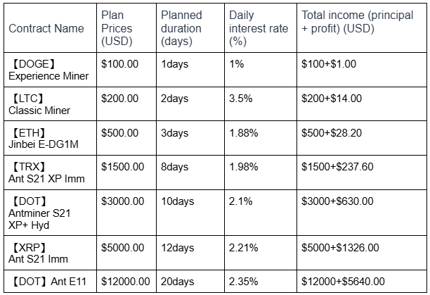
- After the user purchases the mining contract, the real-time data provided by the platform can be used to monitor the mining progress and income.
- Invite and recommend reward mechanism, users can get an additional 7% reward by inviting friends to join the platform.
Core features: simple and efficient, available to everyone
The biggest highlight of DN Miner is its “one-click operation” design. Whether it is a novice user or an experienced miner, it only takes a few simple steps to complete the setup and start of the mining process. In addition, the software is compatible with a variety of hardware configurations, supports mainstream graphics cards and ASIC mining machines, and ensures that users can make full use of existing resources for mining.
Applicable people: From individuals to enterprises, everyone can benefit
DN Miner’s target users cover a wide range, from individual investors interested in cryptocurrency, to small and medium-sized enterprises that want to optimize the mining process, to professional mining pool operators, all of which can use this tool to improve efficiency and reduce operating costs.
Potential advantages: regulatory protection and technological innovation coexist
It is worth mentioning that DN Miner is regulated by the UK Financial Conduct Authority (FCA). This not only reflects its compliance, but also provides users with higher trust and security.

Industry impact: Promote the development of the mining ecosystem
As the cryptocurrency market continues to grow, the mining industry is also facing the challenges of technological complexity and rising costs. The launch of DN Miner has undoubtedly injected a fresh force into the industry. By lowering the technical threshold, it will attract more ordinary users to join the mining ecosystem, thereby promoting the healthy development of the entire industry.
DN Miner is a software solution focused on cryptocurrency mining. Its design concept is to simplify processes, improve efficiency, and provide users with a safe and reliable mining experience. In the future, DN Miner will continue to optimize product functions and create more value for users.
Company name: DNMiner
Company email: info@dnminer.com
Company website: https://dnminer.net
About Author
Disclaimer: The views, suggestions, and opinions expressed here are the sole responsibility of the experts. No Digi Observer journalist was involved in the writing and production of this article.


Empowering Secure and Innovative Investments through AI and Blockchain Integration
Aiden Labs stands at the forefront of technological innovation, merging AI with blockchain to transform how investments and content creation are managed in the digital age. This integration enhances user experiences and investment outcomes through smart, secure, and efficient AI-driven tools.
Aiden Labs: Where AI Meets Web3
Aiden Labs is pioneering the convergence of AI and blockchain through an innovative AI agent platform that allows users to access multiple AI models (ChatGPT, Claude, Gemini) via a single, intuitive interface. This platform not only facilitates creative content generation but also smart crypto investments, all guided by Skynet security ratings from CertiK. Our mission is to democratize access to these powerful technologies, making them accessible for all users while ensuring safety and efficiency in digital transactions and content production.
Core Innovation
Lunar, an AI-powered investment advisor, uses advanced language models and CertiK’s security framework to provide real-time, secure investment insights and analysis.
The Aiden Launchpad Experience Our innovative NFT-powered Launchpad redefines token launches by rewarding community engagement. Through our partnership with BNB Chain, we’ve created a platform where NFT ownership unlocks enhanced allocation opportunities, fostering a deeper connection between projects and their communities.
-
Advanced AI Platform
AI Content Creation Hub Transform your ideas into reality with our suite of AI-powered content creation tools. From generating stunning visuals to crafting engaging videos, our platform empowers creators while ensuring true ownership through blockchain integration.
Recent Achievements
150k+ participants in Aiden Quest Season 1
Secured AA rating on CertiK Leaderboard
Recognized as a Top Growth AI project on BNB Chain and CeritiK Community
Strategic Partnership
Aiden Labs fosters strong partnerships, built upon the BNB Chain and supported by leading blockchain and AI technology providers.
Token Launch Details
- Token Generation Event (TGE): April 7, 2025
- Private Round: $4M, with a 6-month cliff and 12-month linear vesting.
- Public Round: $1M, with 8.33% available at TGE and the remainder vesting over 12 months.
- Initial Market Cap: $3.4M
- Key Backers: Include Crossmint, Mirae Biz Korea, Vsion Inc, QRT Co., Ltd, EugeneFN, Ecogram, and LAON People.
Future Plans: Q2 2025
As Aiden Labs advances into Q2 2025, we are focused on expanding our technology offerings and enhancing our services:
-
Lunar Agent Evolution
-
On-Chain Data Integration: We’re expanding Lunar’s capabilities to include comprehensive on-chain data analysis for crypto projects, providing users with deeper insights and more accurate investment recommendations.
-
Airdrop Hunting Feature: Leveraging our partnerships with blockchain infrastructure providers, we’re developing an intelligent airdrop hunting system within Lunar to help users discover and participate in promising token distribution events.
-
Aiden AI Platform Expansion
Building on our Q1 partnerships, we’ll be significantly enhancing our AI Platform capabilities through:
- Advanced generative AI tools for content creation
- Enhanced security ratings implementation
- Improved cross-chain compatibility
- More intuitive user experiences for both technical and non-technical users
These Q2 developments will further solidify Aiden Labs’ position at the intersection of AI and Web3, creating tangible utility for our growing community of users.
About Aiden Labs
Aiden Labs connects AI & DeFi through AI-agent, delivering an AI Platform, smart investment advice, project ratings & NFT-powered Launchpad. Built with Crossmint & LAON people, backed by CertiK & BNBChain, we’re creating an ecosystem where sophisticated AI agents revolutionize how users interact with blockchain technology.
Connect with Aiden Labs:
Website | X (Twitter) | Telegram | Discord
Join Aiden Labs in building the bridge between AI and Web3, where advanced AI tools meet secure blockchain innovation.
About Author
Disclaimer: The views, suggestions, and opinions expressed here are the sole responsibility of the experts. No Digi Observer journalist was involved in the writing and production of this article.
Electronics manufacturing involves assembling delicate and intricate components like boards of circuitry, microchips, and processors. These components are very susceptible to electrostatic discharge (ESD), which can adversely affect their functionality. ESD is the result of a sudden transition from one object to another with different electrical properties, this can occur simply by walking on a carpet or touching a metal surface. Even a small amount of static electricity can adversely affect electronics that are sensitive, this can lead to product failure and costly repairs.
This is where ESD fabric comes into play. Designed specifically to protect electronic components from static discharge, ESD fabric has become a crucial tool in electronics manufacturing. In this article, we will discuss the top five benefits of using ESD fabric in electronics manufacturing, and why it is indispensable in creating a safe and efficient production environment.
1. Protects Sensitive Electronics from Damage
The primary purpose of utilizing ESD fabric in the electronics industry is to shield delicate electronic components from the adverse effects of static electricity. As we previously mentioned, even a small amount of static pressure can adversely affect or destroy components, leading to costly failures and data loss. Microchips, processors, and other important electronic components can be permanently affected by ESD.
The ESD fabric facilitates this by safely transferring the static electricity to the ground before it reaches the vulnerable components. It prevents the development of static electricity on the surface and the handling of the parts by personnel. Static electricity is dissipated or absorbed by the fabric’s static charge, the mat’s static charge is dissipated or absorbed by the parts themselves, or the entire thing is wrapped in static-resistant fabric and then placed on the employee’s clothing. This is of special significance in areas like clean rooms or assembly lines, where the smallest shock can lead to significant issues.
Brands like LEENOL, a leading “ESD TOTAL SOLUTION” company, offer a comprehensive range of ESD solutions such as LeePak packing materials, LeeRack handling storage, and LeeStat testing equipment to protect sensitive components throughout the manufacturing process.
2. Enhances Manufacturing Efficiency
Another significant benefit of using ESD fabric in the electronics industry is that it increases the overall efficiency of manufacturing. In environments with precision-focused components, minimizing ESD-related damage is critical. If a component is corrupted due to electrostatic discharge, manufacturers must replace the component and potentially restart the manufacturing process, which is both time-consuming and expensive.
By using safety equipment like anti-static clothing, wristbands, mats, and other protective items, the entire manufacturing process is simplified and more efficient. LEENOL, with its extensive ESD product line, provides essential tools such as ESD workbenches with table mats, ESD chairs, and even ESD clothing to ensure that workers can handle electronic components safely.
Moreover, incorporating ESD fabric into packaging solutions, such as ESD bags and trays, helps protect components during transport and storage, ensuring they remain safe from static-related damage throughout the manufacturing process.
3. Cost-Effective Protection
The cost of replacing damaged electronic components due to electrostatic discharge can be astronomical. Components like microprocessors, circuit boards, and memory chips can cost hundreds or even thousands of dollars. When factoring in additional costs like labor, downtime, and repairs, the financial burden becomes even more significant.
ESD fabric offers a cost-effective way to prevent such expenses by protecting components before static discharge happens. By implementing ESD-safe practices early, manufacturers can save money in the long run. LEENOL’s products, manufactured according to international standards like ISO 9001 and ROHS, offer durable and long-lasting protection for electronics manufacturing, ensuring high-quality products are produced with fewer risks.
4. Compliance with Industry Standards and Regulations
In the electronics industry, there are strict regulations governing the handling and protection of sensitive components. These standards are critical to ensuring product safety, reliability, and longevity. Regulations like ANSI/ESD S20.20 and IEC 61340-5-1 set requirements for controlling electrostatic discharge in manufacturing environments.
Using high-quality ESD products like those offered by LEENOL ensures compliance with these standards. Their products, which include ESD clothing, ESD mats, and testing tools, allow manufacturers to meet industry requirements, avoid fines, and demonstrate their commitment to producing safe, high-quality products.
5. Improves Workplace Safety and Employee Comfort
While ESD fabric is designed primarily to protect electronics, it also contributes to a safer and more comfortable work environment. In high-tech manufacturing, employees need to handle components carefully, and their safety is a priority. By wearing ESD garments such as jackets, gloves, and wrist straps, employees protect both themselves and the electronics from electrostatic build-up.
Brands like LEENOL also prioritize worker comfort by offering lightweight and breathable ESD garments, ensuring that employees can work long hours without discomfort. Comfortable employees lead to better performance and higher productivity, reducing the risk of mistakes and improving overall efficiency in manufacturing environments.
How to Implement ESD Fabric in Electronics Manufacturing
Implementing ESD fabric into electronics manufacturing requires careful planning. Here’s how you can integrate it effectively:
* Identify ESD-sensitive areas: Determine where static discharge could impact electronic components, such as assembly lines or cleanrooms.
*Use ESD Garments: Ensure employees handling electronic components are wearing appropriate ESD-safe clothing.
*Install ESD Mats and Work Surfaces: Equip workstations with ESD mats or grounded surfaces to prevent static charge accumulation.
*Ensure Proper Grounding: All ESD equipment must be properly grounded to dissipate static charges safely.
*Regular Maintenance and Training: Regularly inspect ESD fabric and provide ongoing training for employees.
Conclusion
Using ESD fabric in electronics manufacturing is a crucial step in protecting sensitive components, enhancing manufacturing efficiency, and reducing costs. By preventing the damage caused by electrostatic discharge, manufacturers can produce high-quality, reliable products that meet industry standards and regulations. Additionally, incorporating ESD fabric improves workplace safety and employee comfort, creating a positive and productive environment.
Whether you are working in a small repair shop or managing a large electronics manufacturing facility, investing in ESD fabric is essential for safeguarding both your products and your employees. Its effectiveness, affordability, and versatility make it an indispensable tool in the world of electronics manufacturing.
- P.: +86-13818028193 (WhatsAPP)
E-mail: sales@leenol.com
Skype: michellejiangmyskype
Website: https://www.leenol.com/
About Author
Disclaimer: The views, suggestions, and opinions expressed here are the sole responsibility of the experts. No Digi Observer journalist was involved in the writing and production of this article.
Seize the opportunity, DN Miner allows you to easily earn dollars
Why are we bullish? Lunar DeFAI Agent for Investment & Creation from Aiden Labs
Top 5 Benefits of Using ESD Fabric in Electronics Manufacturing
Bay Smokes Maintains Quality Amid Legislative Changes in the Hemp Industry
Benzinga Money Article Discusses How to Become Part of the 12% of Retirees Who Have Achieved the Recommended $550,000 Minimum Retirement Savings Threshold
Apu Apustaja Conquers New York with Lively Street Ads, Including Times Square Billboard


-
Press Release1 week ago
Seospidy CEO Rahul Sharma Honored with Digital Excellence Award 2025 at Global Icon Awards Ceremony
-
Press Release1 week ago
NEKO Reborn: The Catcoin Slayer Unleashes Fun, Value, and Trust in a Community-Driven CryptoRevolution
-
Press Release1 week ago
SIX MINING Launches Remote Crypto Mining Contracts Amid Rising Demand for Accessible Investment Solutions
-
Press Release2 days ago
Digi-Peak: Empowering Users to Create a Safer Digital Cryptocurrency Environment
-
Press Release6 days ago
Dubai-Based Broker Kamil Magomedov Completes Record Sale of Three Entire Buildings in Under Seven Hours Amid Escalating Demand at Expo City
-
Press Release1 week ago
Trading Reimagined: KlasFX Upgrades User Experience with Investor-First Approach
-
Press Release6 days ago
Macmillan Lawyers and Advisors Specialises in Drone Law Services in Brisbane
-
Press Release1 week ago
Lilysuck: Where Genuine Pleasure Encounters Uncompromising Quality